The Ultra-Low Carbon Alliance is excited to announce the launch of a new Q & A series highlighting our members contributions to Ultra Low-Carbon Solar! First, we spoke with Dr. Carsten Rohr from NorSun.
Member Profiles – Dr. Carsten Rohr and NorSun
Carsten Rohr is VP of Business Development at NorSun AS, a manufacturer of premium mono-crystalline silicon wafers based in Norway. Before he started at NorSun in 2007, he was a senior analyst in the Sustainable Energy Analysis team in the UK Government Department for Environment. Previously, Carsten worked as a research associate at Imperial College London in the Centre for Energy Policy and Technology (ICEPT) on the hydrogen energy economy and before that in the Department of Physics on photovoltaic research, including his Ph.D.
This interview has been lightly edited for length and clarity.
Tell me a little bit about your business and where NorSun sits in the solar value chain.
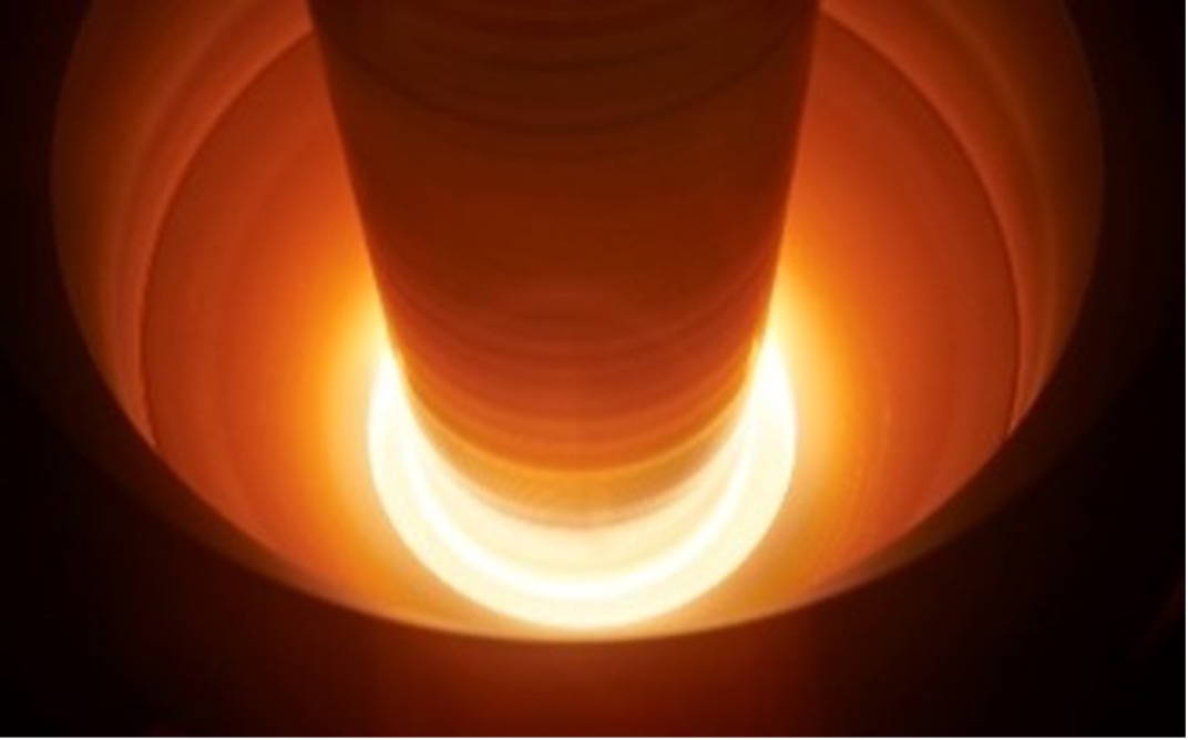
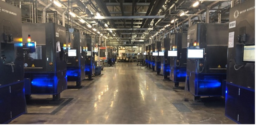
NorSun manufactures premium monocrystalline silicon ingots and wafers, with production facilities in Årdal, Norway. NorSun is currently expanding its capacity from 450 MW to around 1 GW, and has plans to expand further to a total of 4-5 GW at the current site within the next few years. Our customers use our silicon wafers to produce high efficiency, low carbon footprint solar cells and modules.
Congratulations on being the first solar wafer producer to receive the Environmental Product Declaration certifying the low carbon footprint of your products. Tell me a little bit about the EPD.
The Environmental Product Declaration (EPD) is globally recognized and independently verified and registered documentation of the embodied carbon in our products. We are proud to be the first company to receive this EPD for solar wafers. The EPD is compliant with Product Category Rules NPCR 029, v1.1 (EPD Norge) based on international standards ISO 14044, ISO 14025 and EN 15804. EPDs communicate transparent and comparable information about the life-cycle environmental impact of products. We have noticed an increasing interest in the carbon footprint and environmental performance of PV modules and components, but there was no methodology to account for this in a proper way, for example, in construction and building projects. Together with the Norwegian Energy Cluster, Asplan Viak and other stakeholders, we initiated the creation of the EPD Product Category Rules for PV to address this; the EPD PCR was published last year and we then developed the EPD for NorSun’s wafers. With the EPD PCR in place, PV modules can now properly contribute to the carbon footprint and environmental performance of a project, and it is now possible to specify carbon footprint and environmental performance criteria for PV products for example, in tenders and when commissioning projects. We look forward to this solar EPD helping companies specify low carbon solar products in their purchasing.
Silicon ingots and wafers are quite energy intensive to produce. Tell me how you manage to make them with such low embodied carbon. Is it the energy you use, the efficiency of your operations, your supply chain?
NorSun’s wafers have one of the lowest carbon footprints in the world, and to get there requires all of the elements you mentioned. Our production is based on hydropower which has of course essentially no carbon emissions, and we also have plenty of naturally available cooling water, which means that we can reduce our energy consumption by avoiding the use of chillers. In terms of raw material, we use polysilicon from Hemlock (USA) and Wacker (Germany, USA) which has a much lower carbon footprint than the Chinese alternatives (which are largely based on electricity from coal). In addition, by sourcing our polysilicon from these companies we avoid any potential issues with forced labor in the polysilicon industry in the Xinjiang province of China.
In addition to the use of hydro power and careful sourcing of polysilicon, can you say more about the other steps you take to minimize embodied carbon in your wafers?
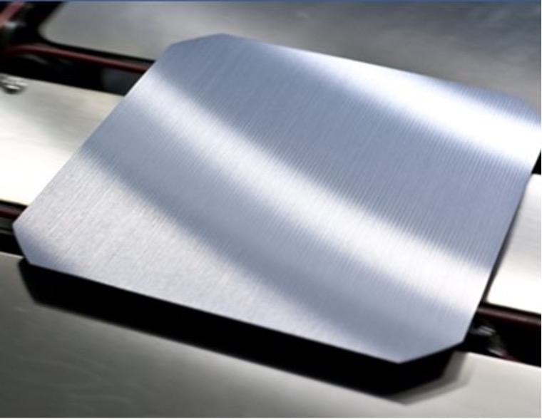
Reducing material consumption contributes to reducing the carbon footprint. For slicing wafers, we use very thin diamond wire to reduce the amount of kerf (essentially polysilicon sawdust) and we produce very thin wafers from the silicon ingots. NorSun’s premium wafers enable high-efficiency solar cells which improves the carbon footprint per kWp and per kWh of the finished solar modules. Furthermore, we have an efficient silicon recycling process.
How do NorSun ingots and wafers help your customers produce Ultra Low-Carbon Solar cells and modules?
Making silicon ingots and wafers is energy intensive. Through the use of polysilicon with low embodied carbon, running our plants on hydropower and high operational efficiency we provide premium low carbon footprint wafers that enable our customers to offer high-efficiency low carbon footprint cells and modules. Many customers are also keen to have a non-Asian alternative for their supply chain.
Are you seeing growing market interest in your ingots and wafers because of their low embodied carbon? For example, I notice you recently announced a new SunPower module from Maxeon powered by NorSun wafers.
SunPower and Maxeon Solar Technologies, who split off from SunPower last year, have been NorSun’s main customer since the beginning in 2007, and we have been supplying low carbon footprint solar materials for PV modules to serve the French tender market in many years as the French government considers the embodied carbon of modules in its tender rules. As we are seeing increasing interest in low carbon footprint PV modules and components also in other market segments, a new SunPower low CO2 footprint module from Maxeon was recently launched powered by NorSun’s Wafers, initially targeting the Scandinavian market.
The French tender system has been pioneering in valuing low carbon footprint for several years now. A similar system has been implemented in Korea last year. The awareness of embodied carbon is increasing and will be taken into account more and more. NorSun is contributing to that development through the efforts on the EPD PCR for example and being a founding member of the Ultra Low-Carbon Solar Alliance (ULCSA) and the European Solar Manufacturing Council (ESMC). In addition, the European Commission is assessing policy instruments such as Eco-design and Energy labeling for PV modules, and there is increasing interest in including relevant criteria in public tenders (Green Public Procurement) and PPAs. Embodied carbon or scope-3 emissions are increasingly becoming part of CSR/climate reporting. These are all promising signs of the growing awareness that we need to make sure that we manufacture clean energy products in a way that is itself clean.
Is there anything that you would like to see change in the solar industry in the next decade?
Solar PV is quickly becoming the most important global energy source as the International Energy Agency acknowledges, and local/domestic/regional production including the entire value chain is therefore strategically important. The PV industry needs to have more focus on the environmental footprint and social issues of PV supply chains and to ensure those supply chains are more secure and resilient. This is increasingly demanded by solar customers and should be supported by policy developments.